How a CD4017 Decade Counter Works: Inside the Internal Circuit Diagram
What the CD4017 Actually Does
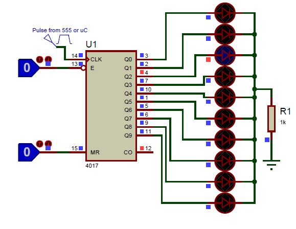
The CD4017 is a CMOS‑based decade counter, meaning it steps through ten distinct states on each clock pulse. In practice, you feed it a square‑wave clock and watch the “Q” outputs light up one after another, from Q0 to Q9. Once it reaches the tenth state, it automatically resets to the first, creating a reliable sequence for everything from LED chasers to motor control.
Because it’s built on CMOS technology, the chip offers very low power consumption and can tolerate a wide voltage range (3 V to 15 V). That flexibility is why hobbyists and designers still reach for the 4017 decades after the first microcontrollers arrived.
Breaking Down the Internal Circuit Diagram
A quick glance at the schematic can feel overwhelming, but the layout falls into a few recognizable blocks:
- Clock Divider – a pair of NAND gates that shape the incoming clock edge.
- Flip‑Flop Chain – ten JK‑type flip‑flops linked in series, each representing one of the ten states.
- Reset Logic – a set of gates that force the counter back to zero when the tenth output or an external reset pin is asserted.
- Enable/Carry Network – controls whether the counter advances or holds its current state.
Clock Divider and Edge Detection
The first two gates form a simple edge‑detector. The clock input (pin 14) is fed into a NAND gate whose other input ties to the previous clock stage, producing a clean, debounced transition. This ensures the flip‑flops only see a single rising (or falling, depending on configuration) edge, preventing accidental double‑counts.
Flip‑Flop Chain – The Heartbeat of the Counter
Each JK flip‑flop is wired in toggle mode: J and K are permanently tied high. With every valid clock edge, the current flip‑flop toggles, while the next one in line receives the carry‑out (the Q̅ of the present stage). This cascading effect is what creates the “one‑hot” sequence—only one Q output is high at any given time.
Because the flip‑flops are identical, the diagram repeats ten times. The only differences are the connections to the reset network and the fact that the final stage (Q9) feeds back to the reset pin (pin 15) through a dedicated gate.
Reset Logic – Returning to Zero
Two situations trigger a reset:
- When the external reset pin is pulled high.
- When the internal Q9 output goes high.
Both signals converge on a NAND gate that drives the master reset line. When either condition is true, the gate forces all flip‑flops back to their initial state, so Q0 becomes high again.
Enable and Carry Controls
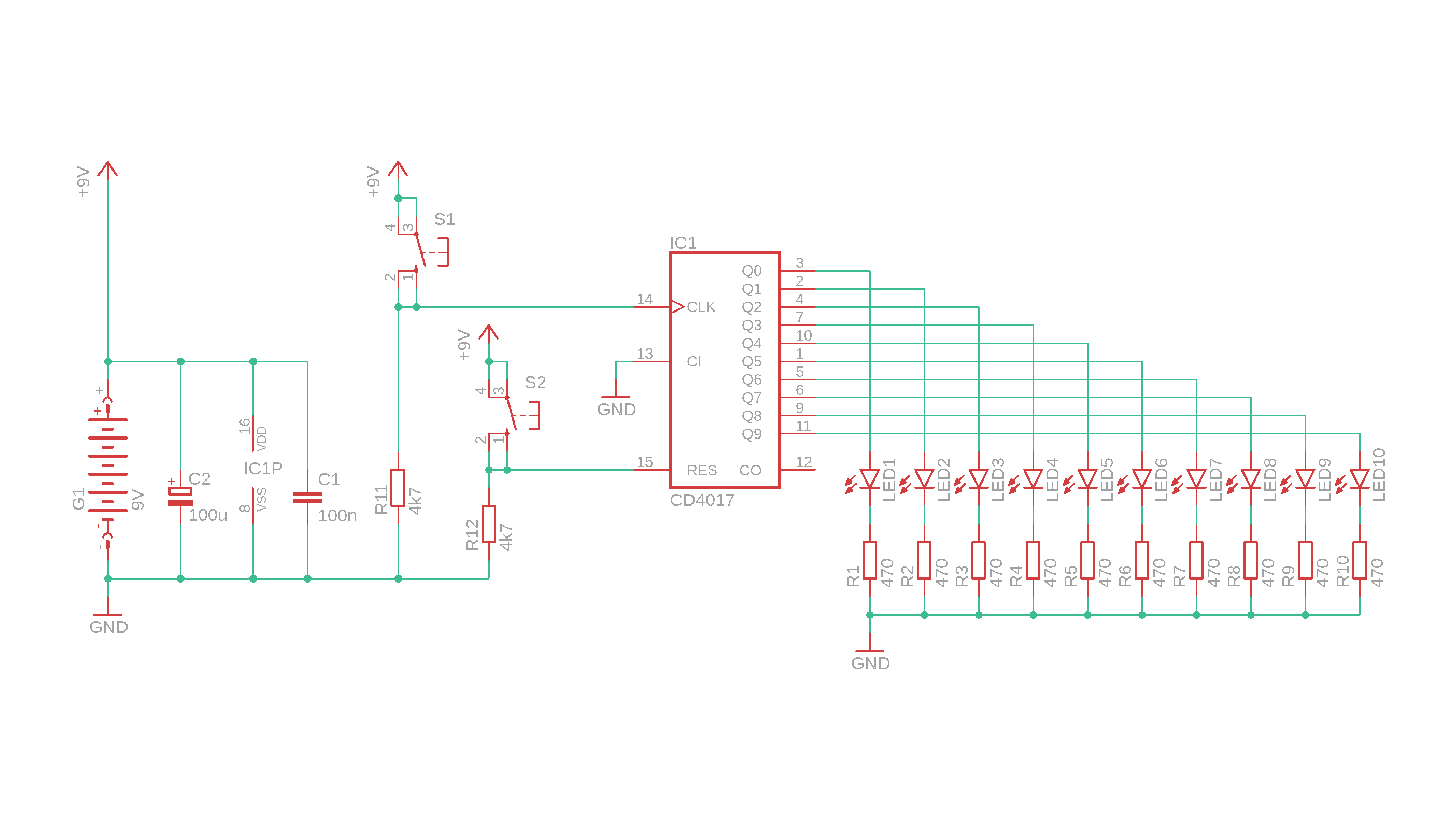
The enable (pin 13) and carry‑out (pin 12) pins add flexibility without complicating the core diagram. Pulling enable low simply freezes the counter—no clock edges are propagated. The carry‑out is essentially the Q9 output; it can be used to cascade multiple CD4017s for longer sequences.
How the Counter Advances Step by Step
Imagine a clean 5 V clock ticking at 1 kHz. Here’s what happens on each pulse:
- The edge‑detector registers the rising edge and sends a short pulse to the first flip‑flop.
- Flip‑flop 0 toggles, making Q0 go high while Q0̅ goes low.
- The low Q0̅ acts as the clock for flip‑flop 1, but because it’s low, flip‑flop 1 stays unchanged.
- On the next clock pulse, the process repeats, but this time the carry‑out from flip‑flop 0 (its Q̅) goes high, clocking flip‑flop 1.
- Now Q1 becomes high, Q0 drops low, and the cycle continues down the line.
When the tenth pulse arrives, flip‑flop 9 toggles, raising Q9. Simultaneously, the reset NAND sees Q9 high, forcing all stages back to zero—ready for the next round.
Practical Tips for Working with the CD4017
- Power‑up sequencing: Give the chip a moment to settle after you apply VDD. A brief delay (a few microseconds) prevents spurious counts.
- Decoupling capacitor: Place a 0.1 µF ceramic capacitor close to the VDD and VSS pins to filter noise.
- Clock source: Use a clean square wave; a noisy oscillator can cause missed or extra counts.
- Output loading: Each Q output can drive up to ~10 mA. If you need more current (e.g., for a string of LEDs), add a small transistor or MOSFET stage.
- Extending the count: Connect the carry‑out (pin 12) to the clock of a second CD4017 for a 100‑step sequencer.
Common Mistakes to Avoid
Beginners often overlook the reset pin, leaving it floating. An unconnected reset can pick up stray noise and reset the counter unpredictably. The simplest fix is to tie pin 15 to ground through a pull‑down resistor (10 kΩ works well).
Another trap is assuming the chip will automatically start at Q0. Power‑on conditions sometimes leave the counter in an undefined state. A quick manual reset pulse right after power‑up guarantees a known starting point.
Wrapping Up the Diagram
The internal circuit of the CD4017 may look like a dense maze of gates, but once you spot the four core blocks—clock divider, flip‑flop chain, reset logic, and enable/carry network—it clicks into place. Understanding how each piece interacts not only demystifies the chip but also opens the door to clever hacks: custom reset thresholds, synchronized multiple counters, or even using the Q outputs as simple PWM sources.
Next time you wire a LED chase or build a step sequencer, take a moment to trace the path through the diagram. You’ll find that the CD4017’s elegance lies in its simplicity, and that simplicity translates into reliable, predictable performance for countless projects.