How the Semiconductor Roadmap Shapes Future Tech Trends
Why a Roadmap Matters
The semiconductor industry doesn’t evolve by accident. Every node shrink, material switch, or architecture tweak follows a carefully plotted plan that spans years, sometimes decades. That plan—often called the technology roadmap—acts like a GPS for manufacturers, investors, and device designers. Without it, the supply chain would scramble, product launches would miss deadlines, and the whole ecosystem would feel the ripple effect.
In practice, the roadmap is a living document. It balances what’s technically feasible with what the market will actually buy. The result? A clear line of sight from today’s 5‑nm silicon to tomorrow’s quantum‑enhanced processors.
Key Milestones on the Current Roadmap
While every foundry publishes its own timeline, a few universal checkpoints have emerged:
- Sub‑5 nm production. Leading fabs are already shipping chips at 3 nm, with 2 nm on the near horizon.
- Chip‑let integration. Instead of a monolithic die, manufacturers are stitching together specialized modules—memory, compute, and I/O—into a single package.
- Advanced packaging. Fan‑out wafer‑level and 2.5‑D interposers are becoming the norm, cutting latency dramatically.
- Emerging materials. Germanium, silicon‑carbide, and even 2‑D materials like graphene are moving from labs to pilot lines.
Each checkpoint carries its own set of challenges—lithography limits, thermal budgets, and cost spikes—but also opens doors to new applications.
Emerging Technologies That Are Redrawing the Map
Two trends are especially disruptive:
1. Heterogeneous Integration
Think of it as building a LEGO set where every block serves a distinct purpose. By combining CPUs, GPUs, AI accelerators, and even analog blocks on a single substrate, designers can tailor performance without waiting for a single “perfect” process node. This approach also mitigates the diminishing returns of traditional scaling.
2. Beyond‑CMOS Computing
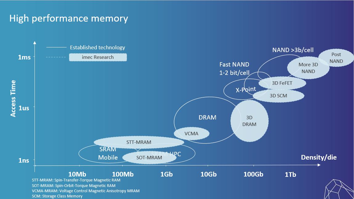
When Moore’s Law starts to plateau, researchers turn to alternatives. Spintronics, photonic interconnects, and quantum bits (qubits) are no longer just academic curiosities. Early‑stage production lines for silicon photonics are already delivering data‑center‑grade links, while spin‑orbit torque devices hint at ultra‑low‑power logic.
Market Implications Across Sectors
Different industries feel the roadmap’s pulse in distinct ways:
- Consumer electronics—smaller, faster chips enable thinner smartphones and wearables with on‑device AI.
- Automotive—robust silicon‑carbide power modules are driving electric‑vehicle range and charger efficiency.
- Healthcare—high‑resolution imaging chips benefit from advanced packaging, delivering clearer diagnostics.
- Data centers—chip‑let designs cut power consumption per FLOP, a critical metric as cloud demand spikes.
Investors watch these shifts closely. A single breakthrough in packaging can shift revenue forecasts for major foundries, while a delay in a new node may ripple through the supply chain, affecting everything from smartphone launch dates to automotive production schedules.
Preparing for the Next Wave
Companies that thrive aren’t merely reacting—they’re anticipating. Here’s a quick checklist for firms looking to align with the upcoming roadmap:
- Build design flexibility: Embrace modular architectures that can swap out a chip‑let without redesigning the whole board.
- Invest in supply‑chain visibility: Real‑time tracking of wafer‑fab capacity helps mitigate bottlenecks.
- Partner with material specialists: Early access to germanium or silicon‑carbide wafers can be a competitive edge.
- Stay agile on software: New hardware capabilities demand optimized compilers and AI frameworks.
Even the “small players” can find niches—think of startups focusing on niche packaging solutions or verification tools for heterogeneous designs. The roadmap isn’t a monolith; it’s a series of opportunities.
Looking Ahead: What Might the 2030s Hold?
Predicting the far future is always a bit of a gamble, but a few educated guesses feel safe:
- 3‑D stacking becomes mainstream. Vertical integration will likely surpass planar scaling as the primary route to density.
- AI‑centric silicon proliferates. Dedicated AI accelerators will be baked into almost every chip, from IoT sensors to high‑end servers.
- Quantum‑ready nodes appear. Not full‑scale quantum computers, but hybrid CMOS‑quantum chips designed for specific cryptographic tasks.
When these trends materialize, the roadmap will have served its purpose: turning speculative research into everyday products, and giving the entire ecosystem a clear direction.