How to Import Gerber Files into EasyEDA: A Simple Step‑by‑Step Guide
Getting a PCB design from a Gerber package into EasyEDA doesn’t have to feel like decoding an ancient script. Whether you’re polishing a hobby project or pulling a layout from a manufacturer’s archive, the process is surprisingly straightforward once you know the right clicks.
Why Bring Gerber Files into EasyEDA?
Gerber files are the lingua franca of PCB production; they describe copper traces, solder masks, and drill data in a series of plain‑text layers. Importing them into EasyEDA gives you a visual playground where you can:
- Inspect every layer for hidden errors.
- Make quick tweaks without opening heavyweight CAD tools.
- Combine existing layouts with new schematics for hybrid designs.
In short, it’s a handy way to double‑check a design before sending it off to a fab, or to revive an old board you found in a drawer.
Preparing Your Gerber Package
Before you even touch EasyEDA, take a minute to confirm that the Gerber files are complete. A typical set includes:
- .GTL – top copper layer
- .GBL – bottom copper layer
- .GTS – top solder mask
- .GBS – bottom solder mask
- .GTO – top silkscreen
- .GBO – bottom silkscreen
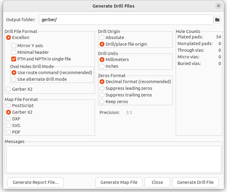
- .DRL – drill data
If any of these are missing, the import will still work, but you’ll end up with a partially rendered board. Double‑check the file extensions, and make sure they’re all stored in the same folder – EasyEDA will look for them together.
Step‑by‑Step Import Process
Now for the fun part. Follow these steps, and you’ll have your design on the canvas in no time.
1. Open a New Project
Log into EasyEDA, click “Create New Project,” and give it a brief, descriptive name. You can leave the default canvas size; it will adjust once the Gerber data loads.
2. Navigate to the Import Tool
On the left toolbar, locate the “Import” icon – it looks like a folder with an arrow. If you can’t spot it, drop down the “File” menu and choose “Import Gerber.”
3. Upload the Files
In the dialog that appears, hit “Select Files” and browse to the folder containing your Gerber set. You can either select them one by one or grab the whole folder; EasyEDA will sort the layers automatically based on their extensions.
4. Confirm Layer Mapping
After the upload, a preview table shows each file and the layer it will occupy. This is your chance to correct any mismatches – for instance, if a silkscreen layer was mistakenly named .GTL. Click the dropdown beside any entry to reassign it.
5. Set Import Options
Most of the time the default settings are fine, but there are a couple of tweaks you might consider:
- Scale factor: If the design was generated in mils but you work in mm, adjust the scale accordingly.
- Origin handling: Choose whether the board origin should be at the lower‑left corner or centered.
6. Finish the Import
Hit “Import.” EasyEDA will process the files and render the board view. Depending on the complexity, this may take a few seconds. When it’s done, you’ll see all layers stacked in the workspace, each togglable from the layer panel on the right.
Fine‑Tuning After Import
The board now lives inside EasyEDA, but you might still want to make adjustments. Here are some common post‑import tasks:
- Align the silkscreen: Sometimes silkscreen text appears slightly offset. Use the “Move” tool to nudge it into place.
- Repair broken traces: If a trace got lost during conversion, draw a new line with the “Track” tool and connect the endpoints.
- Validate drill holes: Switch to “Drill View” and confirm that all holes line up with pads. Missing drills often show as empty circles.
EasyEDA also offers a “Design Rule Check” (DRC) that you can run to catch any clearance violations that slipped through the original Gerber generation.
Exporting Back Out (If Needed)
Once you’ve polished the design, you might want to export it again – perhaps to share with a colleague or to send to a different fab. The process is the reverse of import:
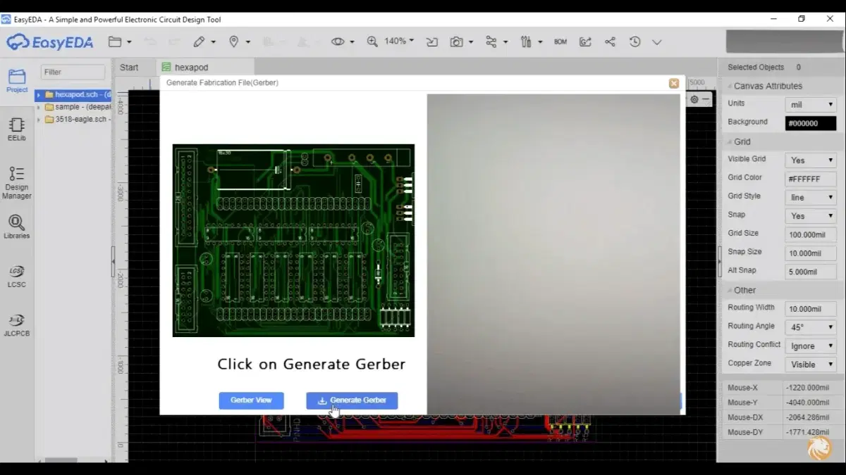
- Click the “Export” button on the top toolbar.
- Select “Gerber” as the output format.
- Choose which layers to include and set the same scale/origin you used during import.
- Download the resulting zip file.
Keep in mind that some advanced EasyEDA features (like custom component footprints) may not translate back into raw Gerber data. If you added such elements, double‑check the exported files before sending them off.
Troubleshooting Common Hiccups
Even with a clean Gerber set, you might run into a snag. Here are a few quick fixes:
- Missing layers: If a layer isn’t showing, verify that its file extension matches one of the recognized types. Renaming .GBL to .GBO, for example, can solve the issue.
- Wrong dimensions: Double‑check the scale factor; a mis‑set factor will make the board appear too large or too tiny.
- Layer order confusion: Use the layer panel to reorder visibility. The top copper should sit above the solder mask, which in turn sits above the silkscreen.
If the problem persists, the EasyEDA community forum is a goldmine of tips – just type the error message into the search bar and you’ll likely find a solution.
Wrapping It Up
Importing Gerber files into EasyEDA is really just a matter of feeding the right files into the right slot and then polishing the result. With the steps above, you should feel confident tackling everything from a simple 2‑layer board to a more intricate multi‑layer design. Next time you have a Gerber package sitting on your hard drive, give EasyEDA a spin – you might be surprised at how much you can achieve without ever leaving your web browser.